Sensorsintermediatecomponent deep dive
ADXL345 at Register Level: I2C vs SPI, Data Rate and Tap Detection
Use the ADXL345 without a library: register map, I2C address, full resolution mode, data rate, offset calibration and tap detection, with Arduino code.
By ADIY14 min read
Technical review pending. Figures marked “verify” or “check your part” have not been confirmed against your exact hardware revision. Check the manufacturer datasheet before relying on them in a design.
Libraries make the ADXL345 easy to read and hard to understand. Working at register level takes an extra hour, and in return you get correct scaling, a data rate matched to your actual signal, and access to the hardware event detection that makes this part worth choosing over cheaper alternatives.
1. Why bother with registers#
A library call returns x, y and z in g. That is genuinely all some applications need. But the library made four decisions for you, and each has consequences:
- Measurement range. Set to ±2 g by default in most libraries. If your application experiences 6 g impacts, every one of them clips silently and you never see the peak.
- Output data rate and bandwidth. Usually left at a default far higher than needed, which admits noise proportional to bandwidth for no benefit.
- Resolution mode. Determines whether your scale factor stays constant when you change range.
- Event detection. Tap, double tap, free fall and activity detection run in hardware and can raise an interrupt. Most libraries never expose them, so people implement inferior versions in software.
That last point is the strongest argument. The ADXL345 can detect a double tap or a free fall condition and assert an interrupt pin while your microcontroller sleeps. Doing the same thing by polling costs you orders of magnitude more power.
2. Choosing the interface#
| Consideration | I2C | SPI |
|---|---|---|
| Signal pins required | 2 shared | 4, of which chip select is per device |
| Devices per bus | Two ADXL345 maximum, via address select | Limited only by available chip select lines |
| Throughput | Adequate to moderate data rates | Higher |
| Wiring complexity | Lower | Higher |
| Susceptibility to bus contention | Shares bus with other peripherals | Independent per device |
| Typical choice for tilt and motion sensing | Recommended | Unnecessary |
I2C address selection#
3. The registers that matter#
The ADXL345 has a substantial register map. These are the ones you will use in practice.
| Addr | Name | Purpose |
|---|---|---|
0x00 | DEVID | Fixed device ID. Reads 0xE5. Your first sanity check. |
0x1D | THRESH_TAP | Tap detection threshold |
0x1E–0x20 | OFSX, OFSY, OFSZ | Per-axis offset trim, applied in hardware |
0x21 | DUR | Maximum event duration to qualify as a tap |
0x22 | LATENT | Wait period after a tap before a second tap can be detected |
0x23 | WINDOW | Window during which a second tap must occur |
0x2A | TAP_AXES | Which axes participate in tap detection |
0x2C | BW_RATE | Output data rate and bandwidth; bit 4 selects low power mode |
0x2D | POWER_CTL | Measure bit (D3) takes the device out of standby |
0x2E | INT_ENABLE | Enable individual interrupt sources |
0x2F | INT_MAP | Route each interrupt to the INT1 or INT2 pin |
0x30 | INT_SOURCE | Which event fired. Reading it clears most flags. |
0x31 | DATA_FORMAT | Range, FULL_RES bit, justification, self test |
0x32–0x37 | DATAX0 to DATAZ1 | Six output bytes, little endian per axis |
0x38 | FIFO_CTL | FIFO mode: bypass, FIFO, stream or trigger |
4. DATA_FORMAT and the full resolution trap#
Register 0x31 controls measurement range and resolution mode, and the interaction between them causes more confusion than any other part of this device.
| FULL_RES bit | Behaviour | Scale factor |
|---|---|---|
| 0 (10-bit mode) | Fixed 10-bit output. Increasing range increases the value each LSB represents. | Changes with range |
| 1 (full resolution) | Bit depth increases with range to hold the scale factor constant. | Approximately 3.9 mg per LSB at all ranges |
5. Output data rate and the noise trade-off#
The BW_RATE register at 0x2C sets the output data rate, and the bandwidth is nominally half that rate. The relationship you need to internalise is simple: wider bandwidth admits more noise. Sampling at 800 Hz when your signal of interest is a person walking gives you a great deal of noise and no additional information.
Set the rate from your application, using the sampling theorem as the floor:
| Application | Signal of interest | Sensible ODR |
|---|---|---|
| Tilt or orientation sensing | Essentially static | 12.5 Hz or below |
| Human activity, step counting | Up to a few Hz | 25 to 50 Hz |
| Tap and gesture detection | Short transients | 100 to 200 Hz |
| Machine vibration monitoring | Depends on machine, often high | Set from your highest frequency of interest, times two, with margin |
6. Offset calibration#
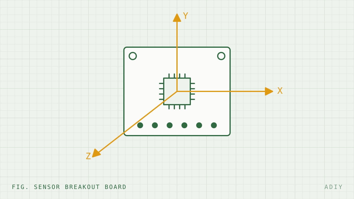
A brand new ADXL345 will not read exactly 0, 0, 1 g when sitting flat. Offsets come from die stress, soldering and board flex, and they are per-device. The ADXL345 provides hardware offset registers, OFSX, OFSY and OFSZ, that are applied to the output automatically, which is neater than correcting in software.
The basic procedure is a six-position calibration: place the board flat, inverted, and on each of its four edges, recording readings at each orientation. In each position one axis reads ±1 g and the other two read 0 g, which gives you both the offset and the sensitivity error for each axis. For many applications a simpler single-position correction with the board flat is sufficient.
7. Complete Arduino sketch#
/*
 * ADIY Labs — ADXL345 register-level driver, I2C
 *
 * Demonstrates: device ID check, full resolution configuration,
 * data rate selection, burst read of all six data bytes,
 * and interrupt-driven single and double tap detection.
 *
 * Wiring (I2C):
 *   VCC -> 3.3V   (check your module; some have an onboard regulator)
 *   GND -> GND
 *   SDA -> A4 on Uno / SDA on other boards
 *   SCL -> A5 on Uno / SCL on other boards
 *   SDO -> GND  (sets address 0x53)
 *   INT1 -> D2  (external interrupt capable pin)
 *
 * NOT bench-verified in this revision. Verify before relying on it.
 */
#include
// SDO to GND = 0x53. SDO to VCC = 0x1D.
#define ADXL345_ADDR    0x53
// Register map
#define REG_DEVID       0x00
#define REG_THRESH_TAP  0x1D
#define REG_OFSX        0x1E
#define REG_DUR         0x21
#define REG_LATENT      0x22
#define REG_WINDOW      0x23
#define REG_TAP_AXES    0x2A
#define REG_BW_RATE     0x2C
#define REG_POWER_CTL   0x2D
#define REG_INT_ENABLE  0x2E
#define REG_INT_MAP     0x2F
#define REG_INT_SOURCE  0x30
#define REG_DATA_FORMAT 0x31
#define REG_DATAX0      0x32
// In FULL_RES mode the scale factor is constant across ranges.
#define SCALE_G_PER_LSB 0.0039   // approx 3.9 mg/LSB
#define INT_PIN         2
volatile bool tapFlag = false;
void writeReg(uint8_t reg, uint8_t val) {
  Wire.beginTransmission(ADXL345_ADDR);
  Wire.write(reg);
  Wire.write(val);
  Wire.endTransmission();
}
uint8_t readReg(uint8_t reg) {
  Wire.beginTransmission(ADXL345_ADDR);
  Wire.write(reg);
  Wire.endTransmission(false);        // repeated start
  Wire.requestFrom(ADXL345_ADDR, 1);
  return Wire.available() ? Wire.read() : 0;
}
// Burst read all six data bytes in ONE transaction. See section 3.
bool readAccel(int16_t &x, int16_t &y, int16_t &z) {
  Wire.beginTransmission(ADXL345_ADDR);
  Wire.write(REG_DATAX0);
  Wire.endTransmission(false);
  Wire.requestFrom(ADXL345_ADDR, 6);
  if (Wire.available() < 6) return false;
  uint8_t b[6];
  for (int i = 0; i < 6; i++) b[i] = Wire.read();
  // Little endian: low byte first for each axis.
  x = (int16_t)((b[1] << 8) | b[0]);
  y = (int16_t)((b[3] << 8) | b[2]);
  z = (int16_t)((b[5] << 8) | b[4]);
  return true;
}
void onTapInterrupt() { tapFlag = true; }
void setup() {
  Serial.begin(115200);
  Wire.begin();
  // --- Step 1: prove the device is there before configuring anything.
  uint8_t id = readReg(REG_DEVID);
  Serial.print("DEVID = 0x"); Serial.println(id, HEX);
  if (id != 0xE5) {
    Serial.println("ERROR: expected 0xE5.");
    Serial.println("Check wiring, pull-ups, and SDO (0x53 vs 0x1D).");
    while (1) delay(1000);
  }
  // --- Step 2: DATA_FORMAT. FULL_RES (bit 3) set, range +/-4g (bits 1:0 = 01).
  //     FULL_RES keeps the scale factor constant. See section 4.
  writeReg(REG_DATA_FORMAT, 0x09);
  // --- Step 3: BW_RATE. 0x0A = 100 Hz ODR, suitable for tap detection.
  //     Lower this for tilt sensing to reduce noise. See section 5.
  writeReg(REG_BW_RATE, 0x0A);
  // --- Step 4: tap detection parameters.
  //     These scale factors are defined in the datasheet; the values
  //     below are a reasonable starting point and WILL need tuning
  //     for your mechanical mounting.
  writeReg(REG_THRESH_TAP, 0x30);   // threshold
  writeReg(REG_DUR,        0x20);   // max duration to count as a tap
  writeReg(REG_LATENT,     0x50);   // gap before 2nd tap allowed
  writeReg(REG_WINDOW,     0xF0);   // window for 2nd tap
  writeReg(REG_TAP_AXES,   0x07);   // enable X, Y and Z
  // --- Step 5: route single and double tap to INT1, then enable them.
  //     INT_MAP bit set = INT2, clear = INT1. 0x00 sends all to INT1.
  writeReg(REG_INT_MAP,    0x00);
  writeReg(REG_INT_ENABLE, 0x60);   // SINGLE_TAP (0x40) | DOUBLE_TAP (0x20)
  // --- Step 6: leave standby. Measure bit is D3 of POWER_CTL.
  writeReg(REG_POWER_CTL,  0x08);
  pinMode(INT_PIN, INPUT);
  attachInterrupt(digitalPinToInterrupt(INT_PIN), onTapInterrupt, RISING);
  // Clear any interrupt latched during configuration.
  readReg(REG_INT_SOURCE);
  Serial.println("ADXL345 ready.");
}
void loop() {
  int16_t rx, ry, rz;
  if (readAccel(rx, ry, rz)) {
    float gx = rx * SCALE_G_PER_LSB;
    float gy = ry * SCALE_G_PER_LSB;
    float gz = rz * SCALE_G_PER_LSB;
    Serial.print("X "); Serial.print(gx, 3);
    Serial.print("  Y "); Serial.print(gy, 3);
    Serial.print("  Z "); Serial.print(gz, 3);
    Serial.println(" g");
  }
  if (tapFlag) {
    tapFlag = false;
    // Reading INT_SOURCE tells you what fired and clears the flags.
    uint8_t src = readReg(REG_INT_SOURCE);
    if (src & 0x20)      Serial.println("** DOUBLE TAP **");
    else if (src & 0x40) Serial.println("** SINGLE TAP **");
  }
  delay(100);
}
Register-level ADXL345 driver with hardware tap detection. Tap thresholds need tuning for your mechanical mounting.
8. Troubleshooting#
| Symptom | Cause | Fix |
|---|---|---|
DEVID reads 0x00 or 0xFF | Wrong address, wiring fault, or missing pull-ups | Run an I2C scanner. Check SDO. Confirm bus pull-ups exist. |
| All axes read zero, DEVID correct | Device still in standby | Set the measure bit (D3) in POWER_CTL at 0x2D. |
| Readings jump between plausible values | Data registers read individually, not as a burst | Read all six bytes in one transaction. |
| Values wrong by a factor of two or four | Range changed without FULL_RES set | Set the FULL_RES bit, or recompute the scale factor for the range. |
| Z does not read about 1 g when flat | Uncalibrated offset | Use the OFSX, OFSY, OFSZ registers. See section 6. |
| Excessive noise | Data rate far above the signal bandwidth | Reduce the ODR in BW_RATE to suit your application. |
| Tap never triggers | Threshold too high, or duration too short | Lower THRESH_TAP, increase DUR. Confirm TAP_AXES enables the axis you are tapping. |
| Tap triggers constantly | Threshold too low for the vibration environment | Raise THRESH_TAP. Secure the module mechanically. |
| Interrupt fires once then never again | INT_SOURCE not read, so the flag stays latched | Read 0x30 in your handler path to clear it. |
FAQ#
What is the I2C address of the ADXL345?
Two selectable addresses. With SDO connected to ground or left unconnected the address is 0x53. With SDO tied to VCC it is 0x1D. This is how you place two ADXL345 devices on one bus. Many breakout boards pull SDO one way by default, so check your board.
How do I verify an ADXL345 is responding?
Read the DEVID register at 0x00. A functioning ADXL345 returns the fixed value 0xE5. If you read 0x00 or 0xFF instead, you have a wiring, address or bus problem rather than a configuration problem. Always do this before writing configuration registers.
What is full resolution mode on the ADXL345?
Set by the FULL_RES bit in DATA_FORMAT at 0x31. The device maintains a constant scale factor of approximately 3.9 mg per LSB across all measurement ranges by increasing bit depth as range increases. In fixed 10-bit mode the scale factor changes with range instead. Full resolution is generally what you want.
Should I use I2C or SPI with the ADXL345?
I2C uses fewer pins and is adequate for most applications up to moderate data rates. SPI supports higher throughput and avoids bus contention, which matters at high output data rates or on a busy I2C bus. For general motion and tilt sensing, I2C is usually the right choice.
Why is my ADXL345 output noisy?
Most commonly an output data rate far higher than the motion you are measuring, which admits noise without adding signal. Lower the rate in BW_RATE to just above twice your highest frequency of interest. Also check the sensor is mechanically secured, since a module on flying leads registers its own movement.
Sources#
Sources and further reading#
- Analog Devices, ADXL345 3-Axis, ±2 g/±4 g/±8 g/±16 g Digital Accelerometer datasheet. Source for the register map, DEVID value, I2C addresses, FULL_RES behaviour, scale factor and the multi-byte read requirement.
- Analog Devices application notes on accelerometer offset calibration using multi-position methods.
Products & resources
Arduino Compatible
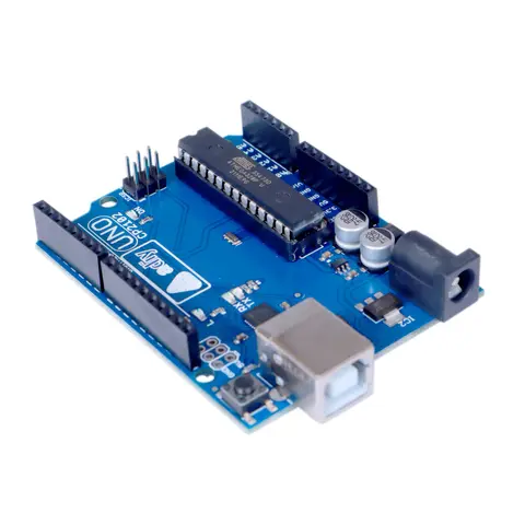
Uno R3 – Compatible CP2102
The ADIY Uno R3 CP2102 ATmega328P Development Board is a cost-effective alternative to the popular Arduino Uno R3. It is designed for beginners and professionals alike, offering robust performance and reliability. Key…
₹552
Datasheet
Share