Powerintermediatedesign notes
LM2596 Design Notes: Thermal Limits, Ripple and When Not to Use It
LM2596 design notes: why the 3 A rating is conditional, thermal derating in Indian ambient, output ripple, input capacitors and better alternatives.
By ADIY12 min read
Technical review pending. Figures marked “verify” or “check your part” have not been confirmed against your exact hardware revision. Check the manufacturer datasheet before relying on them in a design.
The LM2596 is on more Indian prototypes than any other switching regulator, and it is regularly asked to do things it was never specified for. These are the design considerations that separate a module that works on the bench from one that survives a summer in a sealed enclosure.
1. What the datasheet actually says#
| Parameter | Value | Status |
|---|---|---|
| Topology | Non-synchronous step-down (buck) | Datasheet (source stated) |
| Switching frequency | 150 kHz nominal, oscillator tolerance ±15 % | Datasheet (source stated) |
| Input voltage range | 4.5 V to 40 V (standard version) | Datasheet (source stated) |
| Output current capability | 3 A | Datasheet, conditional (source stated) |
| Output voltage tolerance | ±4 % over specified line and load conditions | Datasheet (source stated) |
| Efficiency | Up to approximately 93 %, condition dependent | Datasheet (source stated) |
| Protection | Two stage frequency-reducing current limit, thermal shutdown | Datasheet (source stated) |
Two numbers in that table deserve scrutiny, because they are the ones most often misread.
The 3 A rating is conditional#
The datasheet describes the device as capable of driving a 3 A load. That is a statement about the silicon under specified conditions, including adequate heat sinking. It is not a promise that a 20 mm module with no heat sink will deliver 3 A at any input voltage you choose. Section 2 explains why.
150 kHz is low, and that has consequences#
The datasheet notes that 150 kHz allows smaller filter components than lower frequency regulators, which was true when the part was introduced. Compared to modern converters running at 500 kHz to 2 MHz, 150 kHz is now on the slow side. The practical implications:
- You need a physically larger inductor and more output capacitance for the same ripple
- The control loop is comparatively slow, so transient response to a fast load step is poor
- Switching noise sits in a range where mechanical resonance in ceramic capacitors can become audible as a faint whine
2. Thermal derating, the number that actually limits you#
This is the section that matters most, and it is absent from almost every LM2596 tutorial.
The LM2596 is a non-synchronous buck converter, meaning it uses an external catch diode rather than a second switching MOSFET. Losses come from three places: the internal switch, the catch diode, and the inductor. The dominant term in most applications is the diode, and the loss scales with how much time the diode conducts, which in turn depends on the ratio between input and output voltage.
What this means in an Indian ambient#
Datasheet thermal figures assume a reference ambient temperature. A control panel in Chennai in May, or a sealed junction box on a rooftop, is not that ambient. Internal enclosure temperatures of 55 to 65 °C are ordinary in Indian industrial deployments, and every degree of ambient reduces the headroom you have before thermal shutdown.
Practical guidance:
- Derate hard for a module with no heat sink. Treat a bare small module as a sub-1 A device for continuous duty at a large voltage differential, and validate by measurement rather than by rule of thumb.
- Measure the case temperature under worst-case conditions. Full load, highest input voltage, enclosure closed, hottest expected ambient. Do this before committing to the design, not after the first field failure.
- Leave thermal margin. If the part is running near thermal shutdown on the bench, it will shut down in the field. Thermal shutdown is a protection feature, not an operating mode.
- Consider a two-stage approach for large differentials: step 24 V to 12 V, then 12 V to 5 V. Two converters each doing less work can run cooler in total than one doing all of it, though it costs board area.
3. Capacitor selection#
Capacitor choice is where cheap modules cut corners and where most ripple problems originate.
Input capacitor#
The input capacitor supplies the pulsed current drawn by the switch. It sees high RMS ripple current, and this is a real stress, not a formality. Undersizing it produces input voltage ripple that couples into everything else on the rail, and shortens capacitor life through self-heating.
- Use a low-ESR type rated for the ripple current your application produces
- Place it physically close to the input pin. The loop area formed by the input capacitor, the switch and the catch diode carries fast-edged current, and a large loop radiates.
- Add a small ceramic, typically 100 nF, in parallel for high frequency bypass
- Check the voltage rating with margin. A 25 V capacitor on a 24 V input is not adequate margin once you allow for transients.
Output capacitor#
The output capacitor sets ripple and, critically, participates in loop stability. This is where substituting a "better" capacitor can make things worse.
Bulk capacitance for pulsed loads#
If you are powering something with fast, large current bursts, an LTE module, a Wi-Fi transmitter, a motor, the LM2596 control loop is too slow to respond within the burst. The rail will sag and recover, and your load may brown out during the sag. The fix is local energy storage at the load: bulk capacitance placed close to the device that needs it, not at the regulator output. See our A7670C bring-up guide for a concrete example of this failure mode.
4. Layout notes#
Switching regulator layout is not cosmetic. The same schematic will produce clean or noisy output depending entirely on the board.
- Minimise the high di/dt loop. The path input capacitor, switch, catch diode, back to input capacitor ground carries fast switched current. Keep this loop small and tight. It is the primary EMI source on the board.
- Keep the feedback trace short and away from the switch node. The switch node swings the full input voltage at high speed. A feedback trace routed near it will pick up that noise, and the regulator will faithfully regulate to a corrupted reference.
- Give the catch diode a proper ground connection. A Schottky diode with adequate current rating and low forward voltage is worth the small extra cost, since diode conduction loss is a dominant thermal term.
- Use copper pour for heat spreading. On a module you have limited options, but on your own board the copper area connected to the tab is your heat sink.
- Single-point ground for the feedback divider. Return the divider to the output capacitor ground, not to a random point on the ground pour where switching current is flowing.
5. When not to use the LM2596#
The LM2596 is a well-understood, forgiving, widely available part, and it is the right answer for a lot of prototype and light industrial work. It is the wrong answer in these cases.
| If your requirement is | The problem with LM2596 | Consider instead |
|---|---|---|
| Battery powered, long runtime | Quiescent current and non-synchronous losses hurt at light load | A modern synchronous buck with low quiescent current and pulse skipping |
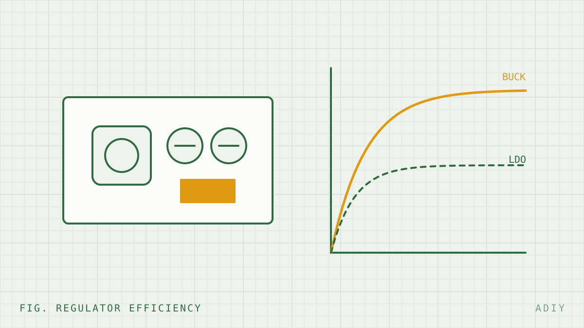
| Low noise analog or RF supply | 150 kHz switching noise couples into sensitive circuits | An LDO, or a switcher followed by an LDO post-regulator |
| Very small board area | Low frequency forces a large inductor and capacitors | A high frequency converter, which shrinks the passives considerably |
| High current with tight thermals | Diode losses generate significant heat | A synchronous buck, which replaces the diode with a MOSFET |
| Small step-down, for example 5 V to 3.3 V | Complexity and noise are not justified | A simple LDO. The dissipation is modest and the output is quiet. |
| Fast transient load | Slow control loop | A faster converter, plus local bulk capacitance at the load regardless |
| Automotive or high transient input | 40 V absolute maximum leaves little margin for spikes | A part with higher voltage rating plus proper input transient protection |
6. Bench validation checklist#
Before you sign off on any LM2596 design, take these measurements. Each one catches a distinct class of failure.
- Output ripple, AC coupled, at full load. Use a short ground spring on the probe, not the long ground lead, which will show you noise that is not there.
- Case temperature at worst case. Highest input voltage, full load, enclosure closed, at the hottest ambient you expect.
- Load step response. Apply a step from light to heavy load and watch the output. Excessive undershoot or ringing indicates a capacitor or loop problem.
- Input voltage sweep. Confirm regulation holds from minimum to maximum input, and note where efficiency and temperature become unacceptable.
- Startup into full load. Some designs regulate fine in steady state but fail to start into a heavy or capacitive load.
- Cold start. If the product will see low ambient temperatures, verify startup there. Electrolytic ESR rises sharply at low temperature.
FAQ#
Can the LM2596 really deliver 3 A?
The device is rated to drive a 3 A load, but that rating is conditional on adequate heat sinking and on the input to output voltage differential. The power dissipated in the regulator rises with that differential, and a typical small module with no heat sink will reach thermal shutdown well below 3 A when stepping down from a high input voltage. Treat 3 A as a silicon capability, not a module capability.
What is the switching frequency of the LM2596?
150 kHz nominal, with an oscillator tolerance specified as plus or minus 15 percent. The relatively low frequency is why it needs a comparatively large inductor and output capacitor, and it places switching noise in a range that can become audible through poorly damped ceramic capacitors.
What is the maximum input voltage for the LM2596?
The standard LM2596 has a maximum input voltage specification of 40 V, and a high voltage variant extends this further. Operating close to the absolute maximum leaves no headroom for input transients, so derate meaningfully below it in any real design.
Why is my LM2596 module getting very hot?
Power dissipated as heat scales with the difference between input and output voltage and with load current. Stepping 24 V down to 5 V at 2 A dissipates far more than stepping 9 V down to 5 V at the same current. Reduce the input voltage if you can, reduce the load, add heat sinking or airflow, or move to a synchronous buck converter.
Is the LM2596 suitable for powering an ESP32 or a 4G module?
It can be, but the deciding factor is transient response rather than average current. Devices with large fast current bursts demand that the rail hold up through a step change in load. The LM2596 has a relatively slow control loop, so adequate bulk output capacitance close to the load is essential. Verify with an oscilloscope during a transmit burst rather than assuming.
Sources#
Sources and further reading#
- Texas Instruments, LM2596 SIMPLE SWITCHER Power Converter 150 kHz 3 A Step-Down Voltage Regulator datasheet (SNVS124). Source for switching frequency, input voltage range, current rating, output tolerance, efficiency and protection features.
- TI application guidance on input and output capacitor selection and layout for the SIMPLE SWITCHER family.
Share